Speeding through the microcosm: Insights into ultrafast electron and lattice dynamics
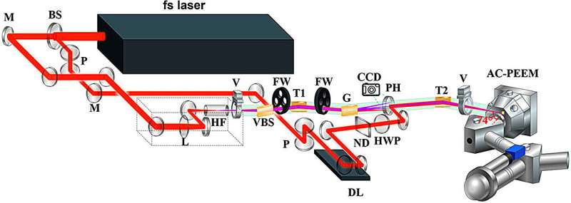
, a reflector (mirror) and an attenuator (ND) to finally reach the sample surface. The figure illustrates that infrared light for pumping and extreme ultraviolet light can be used to excite the surface to produce scattered electrons for detection, while the delay phase (DL) can be adjusted to provide the whole system with a femtosecond to nanosecond time resolution capabilities. . Credit: International Journal of Mechanical System Dynamics (2023). DOI: 10.1002/msd2.12081. Reproduced under the terms of the CC-BY license.87 Copyright 2021, The Authors, published by AIP. BS, beam splitter; DL, delay line; FW, filter wheel; G, grating; HF, hollow fiber; HWP, half wave plate; L, lens; M, reflecting mirror; ND, neutral density filters; P, periscope; PEEM, photo emission electron microscope; PH, pinhole module containing an EUV scintillator; T1, first toroidal mirror; T2, second toroidal mirror 2; V, valve; VBS, vacuum beam splitter.")
Conceptual diagram showing an ultrafast emission electron microscope. The optical path is briefly drawn, with the beam propagating through optical elements such as a partial mirror (BS), a reflector (mirror) and an attenuator (ND) to finally reach the sample surface. The figure illustrates that infrared light for pumping and extreme ultraviolet light can be used to excite the surface to produce scattered electrons for detection, while the delay phase (DL) can be adjusted to provide the whole system with a femtosecond to nanosecond time resolution capabilities. . Credit: International Journal of Mechanical System Dynamics (2023). DOI: 10.1002/msd2.12081. Reproduced under the terms of the CC-BY license.87 Copyright 2021, The Authors, published by AIP. BS, beam splitter; DL, delay line; FW, filter wheel; G, grating; HF, hollow fiber; HWP, half wave plate; L, lens; M, reflecting mirror; ND, neutral density filters; P, periscope; PEEM, photo emission electron microscope; PH, pinhole module containing an EUV scintillator; T1, first toroidal mirror; T2, second toroidal mirror 2; V, valve; VBS, vacuum beam splitter.
A study has unlocked new dimensions in the understanding of ultrafast charge and energy transfer processes at the microscale. The research delves into the dynamics of microscopic particles, providing insights that could revolutionize the development of semiconductors and electronic devices.
Understanding the dynamic behavior of microscopic particles is essential for advancing technologies in various fields, including electronics and materials science. Traditional imaging techniques often fail to capture these rapid processes. Given these challenges, there is an urgent need to develop advanced imaging methods that provide high spatial and temporal resolution to reveal the intricacies of electron and lattice dynamics in materials.
A team from the Beijing Institute of Technology, including researchers from the Laser Micro/Nano Fabrication Laboratory, published a comprehensive review on ultrafast electron microscopy (UEM) in International Journal of Mechanical System Dynamics. This review explores the principles and applications of Scanning Electron Microscopy (TR-PEEM), Ultrafast Scanning Electron Microscopy (SUEM) and Ultrafast Transmission Electron Microscopy (UTEM), highlighting their capabilities in studying ultrafast processes in material.
The review discusses three main UEM techniques: TR-PEEM, SUEM and time-resolved photoemission UTEM. TR-PEEM uses an electron microscope to image the distribution of photoelectron emissions on surfaces, revealing the electron energy distribution and surface plasmon dynamics, and has been used to study heterogeneous interfacial electron transfer and ultrafast electron transport in single-crystal materials.
SUEM combines scanning electron microscopy with ultrafast laser pulses to achieve high spatial and temporal resolution, allowing the observation of carrier dynamics in silicon materials, p–n junction interfaces, and the effects of defect modifications in semiconductor nanowires. This technique is useful in understanding carrier properties influenced by defects, doping, and surface orientation in single crystals.
UTEM offers multiple imaging modes, including real space, inverse space, and energy space, to study lattice dynamics and phase transitions, revealing stress propagation in two-dimensional materials, martensitic phase transformations in metals, and melting processes and crystallization under destructive excitation.
“Ultrafast electron microscopy represents a significant advance in our ability to visualize and understand fast processes at the atomic scale. The insights gained from these techniques are crucial for the development of future technologies in electronics and materials science,” said Professor Lan Jiang, a leader. researcher in this field from the Beijing Institute of Technology.
Advances in UEM techniques have broad implications for scientific research and industrial applications. By providing detailed insights into ultrafast electron and lattice dynamics, these methods can guide the development of advanced semiconductors, optoelectronic devices and efficient photocatalysts. Furthermore, the ability to observe real-time processes at the atomic level opens up new avenues for exploring physics, chemistry and fundamental materials science, ultimately driving innovation in various high-tech industries.
More information:
Yiling Lian et al, Determining electron and lattice dynamics with ultrafast electron microscopy: Principles and applications, International Journal of Mechanical System Dynamics (2023). DOI: 10.1002/msd2.12081
Provided by Maximum Academic Press
citation: Speed through the microcosm: Insights into ultrafast electron and lattice dynamics (2024, June 24) Retrieved June 25, 2024 from https://phys.org/news/2024-06-microcosm-insights-ultrafast-electron-lattice.html
This document is subject to copyright. Except for any fair agreement for study or private research purposes, no part may be reproduced without written permission. The content is provided for informational purposes only.
#Speeding #microcosm #Insights #ultrafast #electron #lattice #dynamics
Image Source : phys.org
Related Posts